Diode, a PN junctionconsists of a combination of two semi-conductor wafers, one of which is doped with tri-valent impurity and the other with penta-valent impurity to make P and N juctions. Both wafers of P and N are not joined by simply pressing them with each other. Rather an intimate contact is necessary. This cannot be obtained by simply connecting them.
Actually in practice, PN junctions are made by using somewhat complex techniques involving simple concepts behind them. We will discuss these techniques one by one. After that we will develop an understanding of the pakaging methods used.
Grown Junctions
This is the most earliest and popular method. This technique employs a method whereby which, PN junctions are actually grown. TRhis is accomplished by placing P-type impurity into a quartz container along with intrinsic semi-conducter wafer. Container is heated in vaccum so that they may not react with atmospheric gases. They are heated util they melt. Small piece of semi-conducter material is then lowerded into the container containing the moiten mixture, know as seed. The molten mixture is allowed to cling with the wafer. For this purpose it is rotated in the mixture and is then brought out of the mixture. This molten mixture finally cools down and becomes hard. This harded material now has the same crystalline characteristics as that of the seed on which it grows.
One may assume that as the molten mixture was p-type so the outer hardened clinged layer must also be the same. But that is not the case. Actually layers of P and N type semiconductors are formed within the region, alternatively. As a result we get a ready made PN junction. These crystals are then sliced to make many PN junctions.
Alloyed Junctions
PN junctions can be made by a technique known as alloyed method. This method is the simplest of all the other. In this method of construction a pallet of tri-valent impurity, Indium is placed on N-type semi-conductor material. This material is then heated at high temparature. The material softens eventually dipping the base of melting pallet into the melting N-type material. Both materials chemically combine to form a PN junction. Indium becomes P-type region. When heat is removed both of them hardens and then recrystallize to form a PN junction ready for slicing.
Diffused Junction Method
This is the most preffered method and the most popular one also. In this technique a thin slice of P-type or N-type material sometimes reffered to as die is exposed to an impurity element in gaseous state at a very high temprature. This type of exposure lets the atoms of impurity to penetrate into the exposed surfaces. And thus results in the formation of PN junction. The gaseous state impurity element belongs to tri-valent group if the slice is N-type semi-conductor or belongs to penta-valent group if the slice is of P-type semiconductor material.
Normally in practice a mask is placed on the N-type semiconductor material before its exposure. It is maked to make the masked suface are unable to go into contact with the gasseous vapours. This inturn allows the limited desired area to go into contact.
The vapours tend to diffuse into the exposed surface of semi-conductor material. The depth of diffusion is controlled by controlling the temparature and time of of contact. More omount of diffusion results into thicker p-type region. This type of diffusion regulation allows making PN junctions (Diodes) of different power ratings.
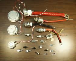
Diode Pakagings
After the formation of PN junctions they are packed in suitable pakaging. Pakaging techniques differ in construction. Pakaging is desired to make the junction safe from envirnomental and other effects like machenical stress etc. Also pakaging is also required to allow different power ratings in construction. For example the PN junction who deals with large amounts of currents should be packed in a container having large surface area to allow the excess heat to escape. In other words we can say that pakaging must be disigned keeping in view the heating effects of the device.
Espacially for heating reduction purposes semiconductor diode is sandwitched between two metal plates usually aluminium and then bolted with nuts of metal. Alumium is commonly used as it has high cofficient of heat. Plates are used to provide more surface area for atmospheric contact. More the exposure to atmosphere is available more the rate of heat escape. Pakages are designed keeping in view all these facts.
PN junction diodes are simplest electronic components and they are commonly used in equipments made for different purposes like avionics, aerospace envirnomentswhere there a chance of heavy stress so it becomes quite inevitable to provide proper protection to enable the components cope with these envirnoments. Moreover devices have to face similar challanges in fields like equpments used in military systems.
That is why suitable pakaging is needed to ensure that components can survive in these envirnoments. For making PN junctions enabled to bear stress, metal casings are commonly used. These casing are typically rounded in shape enclosing semi-conductor device. Leads of cathode and anode are projected outwards from top and bottom providing additional strees bearing ability.

Most common pakaging for PN junction diodes is shown below.
This type of pakaging is commonly used in delicate low power electronic devices most commonly used at homes. This is because it structure does not allows large surfce contact with surrounding making it unable to safely dissipate large amount of heat produced due to the flow of large amount of current. Typically they can handle currents no more than 3 amperes. Small cyliderical glass or epoxy case is used. Leads come out axialy from sides so making it suitable for use in many different configurations on printed circuit board.
Exact package construction of any PN junction diode depends upon its type, Its application and its current bearing capacity. In practice most diode are about 1/4" long and 1/8" in diameter.


0 comments:
Post a Comment